|
No Assembly Required
The PHY is fully tested and verified with state-of-the-art
timing analysis. Through a careful, joint process, the I/O
ring and package are co-designed prior to PHY delivery, so
that the PHY can be fully described, verified and delivered as
a whole. Tremendous flexibility is allowed and no assembly
is required.
Lower Package and Board Costs
Simpler and cheaper (fewer layers) chip packages and
boards can be designed with reduced requirements for
matched trace lengths and more flexibility in the
I/O ring/package co-development.
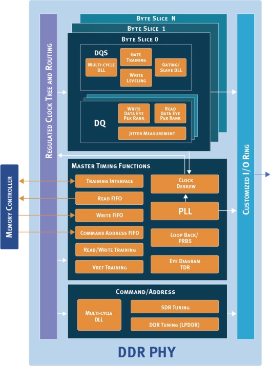
Measurement Resources for Characterization
A special-purpose processor is included in the soft IP component of the PHY and
has been programmed to manage the PHY training operations. Dedicated routines are
executed automatically during the initialization sequence to train the initial
state of the memory system, while other routines can be executed during the
memory system activity, when necessary, to maintain a robust trained state.
The PHY contains many resources that can be set up to quickly characterize a new
chip, a package or a customer's PCB board. Per pin measurements include: DQ
switching jitter, read DQS jitter, read data eye, write data eye, Vref
sensitivity and flight times. Pin and pattern weaknesses can be found quickly,
without expensive lab equipment.
Test
The PHY includes a full speed read/write BIST, which tests
the complete read and write paths of every pin simultaneously
with pseudo-random data. The PHY design kits include
industry-standard boundary scan chains and all the appropriate
views for DFT.
|